
Overview of ESTC 2024 Professional Development Courses on September 11, 2024
Short Courses can be booked together with the conference ticket through our online registration at www.conftool.net/estc2024
8:30 am – 12:45 pm: “Advanced Packaging for MEMS and Sensors”
Course instructor: Horst Theuss
Horst Theuss received his Ph.D. degree in Physics from the University of Stuttgart, Germany in 1993. As a research staff member at the Max Planck Institute for Metal Research he concentrated on magnetic properties of superconductors and amorphous materials. Within a post-doctoral assignment at the IBM Almaden Research Center in San Jose, CA, he worked on magneto-optical properties of exchange-coupled thin layers. In 1996, he started his industrial career at Vacuumschmelze GmbH, Hanau/Germany as a product marketing manager for specialty alloys. Horst Theuss joined Infineon Technologies, Regensburg, Germany in 2000. Since then, he has been working on package concepts and processes in the fields of discrete semiconductors, wafer level packaging, cavity packaging, materials and system integration. As a Senior Principal he is today responsible for predevelopments focusing on MEMS and sensors. Over the years, Horst has continuously contributed to a variety of conferences and magazines with presentations, papers and seminars. He holds more than 100 patents and is co-editor of the “Handbook of Silicon based MEMS Materials and Technologies”.
Course description:
Sensors are everywhere! They create data and provide the “food” for the Internet of Things. Which specific requirements distinguish MEMS and sensor packaging from standard assembly? How are these challenges being tackled? Do we need advanced packaging technologies for MEMS? These are just a few questions which are addressed in the course.
MEMS involve mechanically movable or oscillating parts creating the need for cavity packaging. Concepts for cavity packages are followed by a discussion of package induced stress and its impact to MEMS performance. Among others, respective case studies comprise pressure sensors and MEMS-microphones including a discussion on MEMS-specific materials properties. The advanced packaging section contains an investigation on integrating MEMS-microphones into Fan Out Wafer Level Packages. Robustness requirements and approaches for risk mitigation in harsh environments represent further topics within the PDC’s MEMS section.
The course will go through package requirements of magnetic sensors and stress the importance of advanced packaging for GHz devices – including antenna-in-package technology.
The concluding chapter deals with heterogeneous integration topics. Where is the overlap of the processor-driven world of advanced packaging and the MEMS/Sensor world? Where are the differences and how can we overcome them? A discussion on these topics will be welcome!

08:30 am – 12:45 pm: “Automotive Electronics Reliability – Assurance Approaches and Challenges”
Course instructor: Pradeep Lall
Pradeep Lall is the MacFarlane Endowed Distinguished Professor and Alumni Professor with the Department of Mechanical Engineering. He is the Director of the Auburn University Electronic Packaging Research Institute (AUEPRI), previously CAVE3. He holds Joint Courtesy Appointments in the Department of Electrical and Computer Engineering and the Department of Finance. He is a member of the technical council and academic co-lead of automotive TWG and asset monitoring TWG of NextFlex Manufacturing Institute. He is the author and co-author of 2-books, 15 book chapters, and over 900 journal and conference papers in the field of electronics reliability, manufacturing, safety, test, energy efficiency, and survivability. Dr. Lall is a fellow of the ASME, a fellow of the IEEE, a Fellow of NextFlex Manufacturing Institute, and a Fellow of the Alabama Academy of Science. He is a recipient of the SEMI Flexi R&D Achievements Award for landmark contributions to Additive Printed Electronics, ASME Avram Bar-Cohen Memorial Medal, IEEE Biedenbach Outstanding Engineering Educator Award, Auburn University Research Advisory Board’s Advancement of Research and Scholarship Achievement Award, IEEE Sustained Outstanding Technical Contributions Award, NSF-IUCRC Association’s Alex Schwarzkopf Award, Alabama Academy of Science Wright A, Gardner Award, IEEE Exceptional Technical Achievement Award, ASME-EPPD Applied Mechanics Award, SMTA’s Member of Technical Distinction Award, Auburn University’s Creative Research and Scholarship Award, SEC Faculty Achievement Award, Samuel Ginn College of Engineering Senior Faculty Research Award, Three-Motorola Outstanding Innovation Awards, Five-Motorola Engineering Awards, and over Forty Best-Paper Awards at national and international conferences. Dr. Lall is the founding faculty advisor for the SMTA student chapter at Auburn University and a member of the editorial advisory board for SMTA Journal.
Course description:
The modern car has increased semiconductor content and dollar value. Semiconductors enable the majority of innovations in automotive. The increased emphasis on autonomous driving and the electrification of vehicles has resulted in enormous changes for semiconductors and packaging. The design, materials, and reliability strategies for automotive electronics will be presented. Electronics are increasingly being used in automotive platforms for various mission-critical and safety-critical activities, such as guidance, navigation, control, charging, sensing, and operator interaction. Over the last two decades, automotive platforms have expanded to incorporate hybrid and fully-electric vehicles. Much of the electronics is located under the car’s hood or in the trunk, where temperatures and vibration levels are far higher than in consumer office applications. During the vehicle’s use-life, electronics in the automotive underhood may be exposed to sustained high temperatures of 125-150°C for extended periods of time. The automotive electronics council (AEC) has graded electronics for automotive purposes into four categories: grade-0, grade-1, grade-2, and grade-3. Grade-0 components have the most demanding criteria of the four grade categories, with predicted power temperature cycling ranging from -40°C to +150°C for 1000 cycles and ambient temperature cycling ranging from -55°C to +150°C for 2000 cycles. Furthermore, the grade-0 components are expected to be capable of sustaining high-temperature storage for 1000 hours at 175°C. With the introduction of new packaging architectures, packaging applications have continued to evolve, allowing for powerful computing on mobile automobile platforms. New materials and integration technologies have also emerged, allowing for tighter integration of electronics sensing and processing into the structural characteristics of the vehicle. The automobile platform faces a series of constraints particular to the real-time context for enabling sophisticated functionality.
Specifically, the course will encompass the following topics:
- Role of electronics on the automotive platform
- Automotive environments
- Zero-Defects
- Second-Level Solder Interconnect Design Considerations
- Copper Wirebond Interconnects
- Advanced Packaging Interfaces
- Vibration Effects
- Sustained High Temperature and Wide Thermal Extremes
- Corrosion Propensity
- Accelerated Testing
8:30 am – 12:45 pm: “Flip Chip Fabrication and Applications“
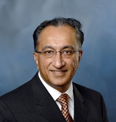
Course instructor: Eric Perfecto
Eric Perfecto has over 41 years of experience working in the development and implementation of C4 and advanced Si packages at IBM and GlobalFoundries. Eric’s responsibilities include UBM and Pb-free solder definition for C4 and u-Pillar interconnect, and yield improvements in C4 and 3D wafer finishing. He holds a M.S. in Chemical Engineering from the University of Illinois and a M.S. in Operations Research from Union College. Eric has published over 80 papers in conferences and journals, including two best Conference Paper Awards and the 1994 Prize Paper Award from CMPT Trans. on Adv. Packaging. He holds 60 US patents and has been honored with three IBM Outstanding Technical Awards. Eric was the 57th ECTC General Chair in Reno, NV, and the Program Chair at the 55th ECTC. Eric is an IEEE Fellow, an EPS Distinguish Lecturer and EPS VP of Education.
Course description:
This course will cover the fundamentals of all aspects of flip chip fabrication and assembly technologies. It is divided into two main sections. The first part covers the main type of assembly technologies chip package interaction, package warpage control, yield detractors, substrate technologies, etc. The second dives into the depth of the fundamental aspect of flip chip fabrication mainly; interconnect technologies, under-bump metallurgy selection, fabrication methods and solder depositions methods. The course will cover the various failure modes related to bumping, such as barrier consumption, Kirkendall void formation, non-wets, BEOL dielectric cracking, etc. Special focus of the course will be on fine pitch technologies, mainly u-Pillar and Hybrid bonding. The goal of this course is to provide the students with a better understanding of flip chip and assembly applications so that a reliable, innovative, better time to market, and more cost-effective solution can be achieved.
Course Outline
1. Introduction to Flip Chip Technologies
2. Flip Chip Technologies: Mass Reflow Process
3. Flip Chip Technologies: Thermal Compression
4. Substrate Technologies, Underfill, Package Warpage Control, and Yield
5. Flip Chip Reliability Assessment, Failure Modes, Examples, and Modeling
6. Flip Chip Si Package Co-Design
7. Chip-Package Interaction and Flip Chip Electromigration
8. Flip Chip New Trends: Wafer Level CSP; Wafer Level Fan-Out; and Panel-Level Packaging
9. Fine pitch interconnect options (for <100um pitch)
10. Bumping Ground Rules
11. Flip Chip Under-bump Metal and Intermetallic
12. Flip Chip Solder Deposition Processes
13. Cu Pillar Technology
14. Flip Chip Solder Selection and SLID
15. Hybrid Bonding (for less that 10um pitch)

8:30 am – 12:45 pm: Printed Electronics Technologies in Green Hydrogen Generation and Conversion: principles, methods and applications
Course instructor: Claudia Delgado Simao and Diogo Garcia Esperança (Fundació Eurecat)
Dr. Claudia Simão (PhD 2011) is specialized in functional surfaces with tuned optical, magnetic, mechanical and electric properties. She has coordinated and participated in multiple European and national projects, authored several peer-reviewed publications and patent applications and received several awards for her research. Currently, is a Senior Team Leader and head of the Printed Energy Devices research group at Eurecat – Centre Tecnològic de Catalunya, investigating novel printed electronics solutions and cost-effective large area methodologies for lightweight devices with a particular focus on energy generation and conversion and self-powered sensors.
Dr. Diogo Garcia is a Materials Engineer currently affiliated with the Printed Energy Devices research group at Fundació Eurecat in Barcelona, Spain. He holds an MSc degree in Materials Engineering from the NOVA School of Science and Technology in Portugal, which he completed in 2018. He pursued his Ph.D. as part of a European Joint-Doctorate program. As a Marie-Curie fellow within the eSCALED Project his doctoral research focused on the development of new porous functional materials for photo and electrochemical devices used in artificial photosynthesis and green hydrogen production.
Course description:
This short course probes the intersection of printed electronics and green hydrogen technologies, providing participants with essential knowledge and practical insights into both fields and aims to highlight how printed electronics can enhance various aspects of green hydrogen production and conversion processes. The course covers key principles, state of the art and emerging trends, and real-world applications, offering a specialized focus on the role of printed electronics in advancing sustainable hydrogen generation and conversion methods.
I. Overview of hydrogen production methods
- Importance of renewable energy sources in hydrogen generation
- Environmental and economic considerations in green hydrogen technologies
- Recent advancements in renewable energy integration in green H2 production
II. Basic principles and components of printed electronics
- Printing techniques suitable for green hydrogen applications
- Materials used in printed electronics and their compatibility with sustainable practices
- Future trends and innovations
III. Overview of electrolysis for hydrogen production
- Role of printed electronics in improving electrolysis efficiency
- Innovations and challenges in printed electrolysis components
- Manufacturing processes and eco-friendly considerations
- Smart controls and monitoring systems
IV. Overview of fuel cells for hydrogen conversion
- Role of printed electronics in improving fuel cells efficiency
- Manufacturing processes and state of the art examples
V. Sustainable practices in the production of printed electronics
- Life cycle assessments and eco-design principles for printed electronic components
- Scalability and reproducibility of environmentally conscious printing methods

