The 11th IEEE ESTC
SEPTEMBER 9–11, 2026 | HELSINKI, FINLAND
Keynotes
Wednesday, September 9, 2026, 1:45pm – 2:10pm
6G Wireless Telecommunication challenges to semiconductors and SoCs
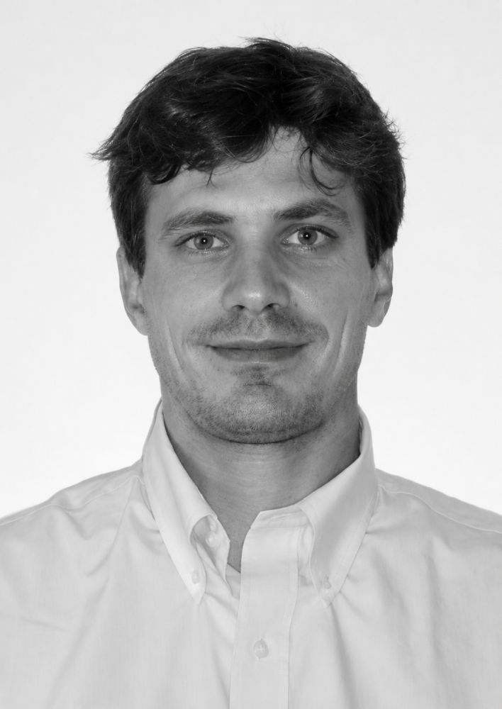
Sami Repo
MN SoC Chief Technology Officer, Nokia Solutions & Networks
Mr. Sami Repo has served as MN SoC Chief Technology Officer at Nokia Solutions & Networks Oy since February 2025. With over 25 years of experience in wireless digital hardware design and embedded systems, he has held key leadership roles in SoC development, architecture, and hardware R&D. Throughout his career, Mr. Repo has worked mainly at wireless telecommunication semiconductor side. First in Nokia Mobile Phones where he began his professional journey and held various positions, as well as at Broadcom and Renesas Mobile Corporation, before joining back to Nokia Networks in 2013. He holds an M.Sc. in Electrical and Information Engineering from the University of Oulu.
Abstract:
A view to 6G Mobile Telecommunications space, with semiconductor needs and challenges in it.

Wednesday, September 9, 2026, 2:10pm – 2:35pm
The Future of Computing – Let's Make It Quantum
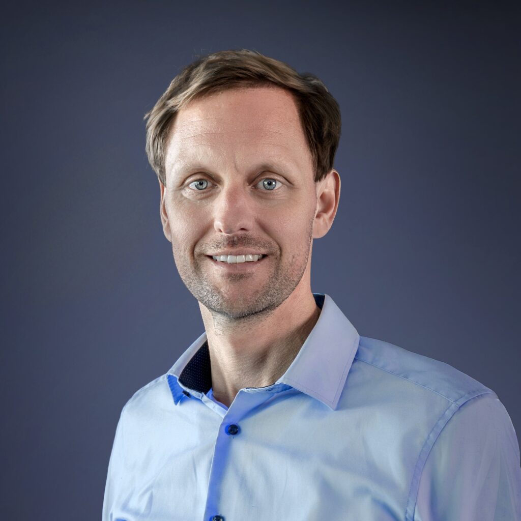
Dr. Jan Goetz
IQM Quantum Computers
Dr. Jan Goetz is the CEO & Co-Founder of IQM Quantum Computers, a global leader in quantum computing. Jan Goetz did his doctorate on superconducting quantum circuits at TU Munich and worked as a Marie-Curie Fellow in Helsinki at Aalto University, where he holds the title of docent. He has raised over $600M of capital for the company together with his co-Founders since the company was founded in 2018. He serves as an EIC ambassador and holds a Board seat in the European Quantum Industry Consortium QuIC. He is a member of the German Federal Economic Senate, EIC Scaling Club Council and the Hall of Future. He is also a Digital Leader and Global Innovator at the WEF.
Abstract:
This talk will describe the current state of quantum computing and roadmaps to achieve commercial quantum advantage.
Thursday, September 10, 2026, 8:30am – 8:55am
Packaging Technology – A Future Enabler for AI and Automotive
Thorsten Meyer, Infineon
Thorsten Meyer is Distinguished Engineer for Package Concept Engineering at Infineon Technologies in Regensburg, Germany, responsible for New Package concepts. Before, he was leading the Package Technology and Innovation department at Intel Mobile Communications (IMC) in Regensburg and earlier was overall project leader for the development of Wafer Level Packaging Technologies at Infineon in Regensburg.
Thorsten is author of multiple publications and holds more than 200 patents and patent applications in the area of advanced packaging.
Abstract:
The acceleration of artificial intelligence and its power supply, the electrification of mobility, and the expansion of the Internet of Things (IoT) are continuously requiring innovations in materials, thermal management, and interconnect technologies. These are becoming critical enablers for next-generation applications in all areas. The talk highlights packaging challenges and opportunities for Power and Automotive Applications.

Thursday, September 10, 2026, 1:15pm – 1:40pm
Next-Generation Silicon Photonics powering future AI Compute
Joris Van Campenhout
Program director optical input/output (I/O), imec
Joris Van Campenhout is Fellow Silicon Photonics and senior director of imec’s industry-affiliation R&D program on Optical I/O, which targets the development of scalable short-reach optical interconnect technology based on silicon photonics. Prior to joining imec in 2010, he was with IBM’s TJ Watson Research Center (USA), where he developed silicon electro-optic switches. He obtained a PhD degree in Electrical Engineering from Ghent University (Belgium) in 2007, for his work on heterogeneous integration of InP lasers on silicon. Joris has been granted 15+ patents and has authored or co-authored over 100 papers in the field of silicon integrated photonics, which have received 15000+ citations.
Abstract:
The scaling of future AI/ML clusters hinges increasingly on pushing optical interconnect technology deep into the system. In this presentation, we will outline our vision for deeply integrating optical interconnects into the package, interposer, and wafer level, leveraging scaled Silicon Photonics, novel materials and advanced 3D technologies to implement high-density sub-pJ/bit optical transceivers. We will share some recent results from our ongoing research and development efforts on advanced optical devices, packaging and assembly.

Friday, September 11, 2026, 9:00am – 9:25am
Advanced Packaging for Chiplets and Heterogeneous Integration
John H Lau
Unimicron Technology Corporation
John H Lau, with more than 40 years of R&D and manufacturing experience in semiconductor packaging, has published more than 530 peer-reviewed papers (385 are the principal investigator), 52 issued and pending US patents (31 are the principal inventor), and 25 textbooks. John is an elected IEEE fellow, IMAPS Fellow, and ASME Fellow and has been actively participating in industry/academy/society meetings/conferences to contribute, learn, and share.
Abstract:
Advanced packaging is ranked based on their interconnect density and electrical performance and grouped into 2D, 2.1D, 2.3D, 2.5D, 3D. 3.3D, and 3.5D IC integrations. Chiplet communication such as bridges embedded in build-up package substrate and in fan-out EMC with RDLs will be discussed. Fundamental of Hybrid bonding will be briefly mentioned and HVM products with hybrid bonding will be presented. HBM and cHBM are one of the key elements of HPC products driven by AI will be discussed. Glass-core substrates and glass-core interposers will be presented. Some recommendations will be provided.
- Introduction
- Chiplets and Heterogeneous Integration
- Advanced Packaging for Chiplets and Heterogeneous Integration
- 2D IC Integration
- 2.1D IC Integration
- 2.3D IC Integration
- 2.5D IC Integration
- 3D IC Integration
- 3.3D IC Integration
- 3.5D IC Integration
- Bridges Embedded in Build-up Substrates
- Bridges Embedded in Fan-Out EMC with RDLs
- Hybrid Bonding Bridge
- HBM vs. cHBM
- Glass Packaging
- Summary and Recommendations
Friday, September 11, 2026, 2:35pm – 3:00pm
Advanced Packaging: Infusing AI at Scale
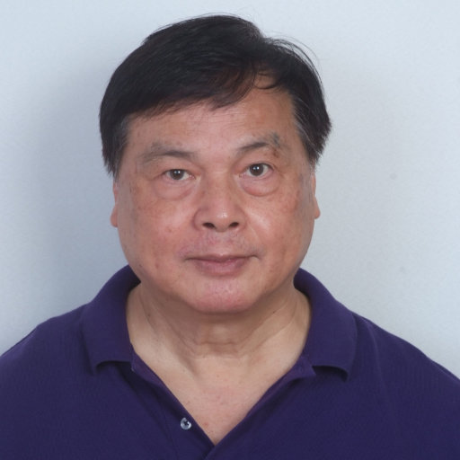
Dr. Christophe Zinck
Director of Technical Program Management, ASE
Dr. Christophe Zinck is Director of Technical Program Management at ASE Europe, where he leads technology teams focused on advanced assembly processes for high-performance digital, power, RF, and MEMS & sensor devices.
He began his more than 20-year career in semiconductors in Grenoble, France, holding various roles at CEA-Leti and STMicroelectronics, where he specialized in lithographic process development. He later joined TriQuint Semiconductors in the United States, driving innovation in advanced packaging for RF devices. Upon returning to France, he contributed to Yole Développement and subsequently managed silicon sourcing activities at SOITEC.
Dr. Zinck has co-authored more than 50 publications, holds several U.S. patents, and is a frequent speaker at international industry conferences. He earned his Ph.D. from the Institut National des Sciences Appliquées (INSA) de Lyon.
Abstract:
As the limits of traditional scaling come into view, advanced packaging is becoming the new frontier of semiconductor innovation. In this keynote, Christophe Zinck will explore how heterogeneous integration, chiplets, and advanced system architectures are enabling the performance, efficiency, and scalability demanded by the AI era, while highlighting the importance of collaboration across the semiconductor ecosystem to turn innovation into industrial reality.
Zinck will share advanced packaging innovations to demonstrate that the future of AI will not be defined by silicon alone, but by what happens around it.