ESTC 2024
Keynotes
Electronics Integration: Challenges in Computed Tomography Scanners
Dr. Michael Hosemann
Head of Digital Electronics at Healthineers Computed Tomography Detector Center, Siemens
Dr. Michael Hosemann is the Head of Digital Electronics at Siemens Healthineers Computed Tomography Detector Center. This spans a range from front-end mixed-signal ASIC development via PCB design, firmware development for ASIC control, data processing to wireless data transmission. Michael did his Diplomingenieur and doctorate degrees at Technische Universität Dresden. Before joining Siemens Healthineers he worked for a variety of companies in Cambridge, UK and Germany, mainly designing wireless and medical systems.
Abstract:
Medical devices pose a large spectrum of challenges for integration of electronics components.
This talk highlights some of those challenges based on the world’s first photon-counting computed tomography scanner, Siemens Healthinneers’ Naeotom Alpha. Examples include gap-less 3D assembly of detector ASICs to handling measurement data in excess of 500Gbit/s.

Challenges and Opportunities of Semiconductor Packaging in the Chiplet Era
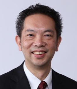
Dr. Yasumitsu Orii
Senior Managing Executive Officer in 3D Assembly Division, Rapidus Corporation
Dr. Yasumitsu Orii joined IBM Japan in 1986, was a pioneering figure in Flip Chip organic packages, enhancing performance and miniaturization in servers, laptops, and HDDs. With Moore’s Law limitations, packaging technology gains significance for next-gen servers. Yasumitsu led innovations such as flip chip on FPC for HDDs and developed C2 technology for low-cost flip chip bonding in consumer electronics, licensed to a Taiwanese firm. At IBM Research Tokyo, he spearheaded projects on 3D-IC and Neuromorphic Computing. After leaving IBM in 2014, he joined NAGASE & CO., LTD., launching material informatics software as a service. He left NAGASE and in December 2022 and joined Rapidus Corporation, where he now serves as Senior Managing Executive Officer in the 3D Assembly Division.
Abstract:
Splitting a System-on-Chip (SoC) chip into individual chips (chiplets) by function brings improved yields, shorter design, development cycles, and cost reduction. However, moving from monolithic chips to chiplets brings forth new challenges in high-density interconnects, thermal management, and testing. Additionally, the packaging structures are becoming more complex, resulting in increased design complexity. To address these challenges, the entire industry should promote the integration of front-end and back-end processes and establish a chiplet ecosystem.

Packaging: then, now and in the future.
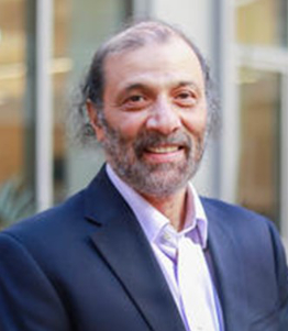
Subramanian S. Iyer
Director National Advanced Packaging Manufacturing Program, CHIPS R&D Office, National Institute of Standards and Technology, Department of Commerce. Los Angeles CA.
Subramanian S. Iyer (Subu) is Director of the National Advanced Packaging Manufacturing Program (NAPMP), on assignment from UCLA where he is Distinguished Professor and holds the Charles P. Reames Endowed Chair in the Electrical Engineering Department and a joint appointment in the Materials Science and Engineering Department at the University of California at Los Angeles. He is the founding Director of the Center for Heterogeneous Integration and Performance Scaling (UCLA CHIPS). Prior to that he was an IBM Fellow. His key technical contributions have been the development of the world’s first SiGe base HBT, Salicide, electrical fuses, embedded DRAM and 45nm technology node and used to make the first generation of truly low power portable devices as well as the first commercial interposer and 3D integrated products. He has been exploring new packaging paradigms and device innovations that may enable wafer-scale architectures, in-memory analog compute and medical engineering applications. He is a fellow of IEEE, APS, iMAPS and NAI as well as a Distinguished Lecturer of IEEE EDS and EPS. He is a Distinguished Alumnus of IIT Bombay and received the IEEE Daniel Noble Medal for emerging technologies in 2012 the 2020 iMAPS Daniel C. Hughes Jr Memorial Award and the iMAPS distinguished educator award in 2021.
List of publications/patents:
https://scholar.google.com/citations?user=xXV4oIMAAAAJ&hl=en
Abstract:
Packaging has evolved from the role of primarily protecting the chip to one of overall system integration of heterogeneous chiplets. An important aspect of this integration is miniaturization. Feature sizes such as substrate wiring pitch, die-to-substrate bonding pitch, and inter-die distances need to shrink in a predictable manner to approach monolithic wiring pitches, last level via pitches and IP block spacings. We refer to this as shrinking down of the package. Simultaneously, we need to increase the number of dies interconnected on the package to improve performance and functionality. We refer to this as scaling out of the package. Current approaches to this include additional levels in the packaging hierarchy with concomitant increases in complexity and cost. We need to think of new ways of flattening the packaging hierarchy by enabling substrates with finer wiring pitches and the ability to assemble dies at fine pitch at high throughput. Besides the technology and processes needed to accomplish this, there are other difficult issues that need to be addressed: these include power delivery and thermal dissipation, high bandwidth, and potentially active wired, wireless, and photonic connectors to the external world or between subsystems. Finally, to make this vision a reality a chiplet eco system needs to be developed with mechanical and electrical standards that ensure interoperability and a high level of reuse. Similarly, a comprehensive EDA approach needs to be developed that goes well beyond electrical abstraction of the system and includes among other things thermal, thermomechanical considerations, power delivery, test methodology and reliability. This is a challenging opportunity and promises to continue the trend set by Moore’s law, for system integration.

